Wei GROUP
Nanofabrication
Lab (MP 087 & 089)
Our nanofabrication facilities consist of:
- Electron beam writer (+ scanning electron microscope)
- Thin-film
processing chamber
- Sputtering guns (DC & RF)
- Ion milling gun
- Thermal evaporator
- Electron beam evaporator
Electron beam
writer for nanolithography
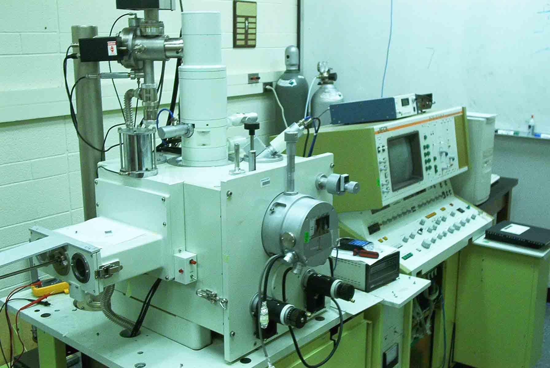
Our electron-beam writer is based on a JEOL-848
scanning
electron microscope (SEM) fitted with a
beam blanker, picoammeter and nano-pattern generation system (Nabity
NPGS) control
electronics & software. It is capable of writing and
imaging with a scanning electron beam, and can achieve resolution down
to ~20nm at 25keV depending on the material and filament used. The
large-volume sample chamber is equipped with a load-lock
hatch for
quick sample exchange and a computer-controlled sample stage for large
travel. An on-board ion pump enables lanthanum hexaboride, intead
of tungsten, filaments to be used for higher resolution in
ultra-high vacuum mode.
Nanolithography is carried out using various electro-resists as masks,
applied by spin coating, defined by scanning electron beam, followed by
chemical etching. In the case of complex oxides, we have
developed a breakthrough method for making nanostructures, using the
principle of selective epitaxial growth in conjunction with pulsed
laser thin-film deposition.
Thin-film
processing chamber
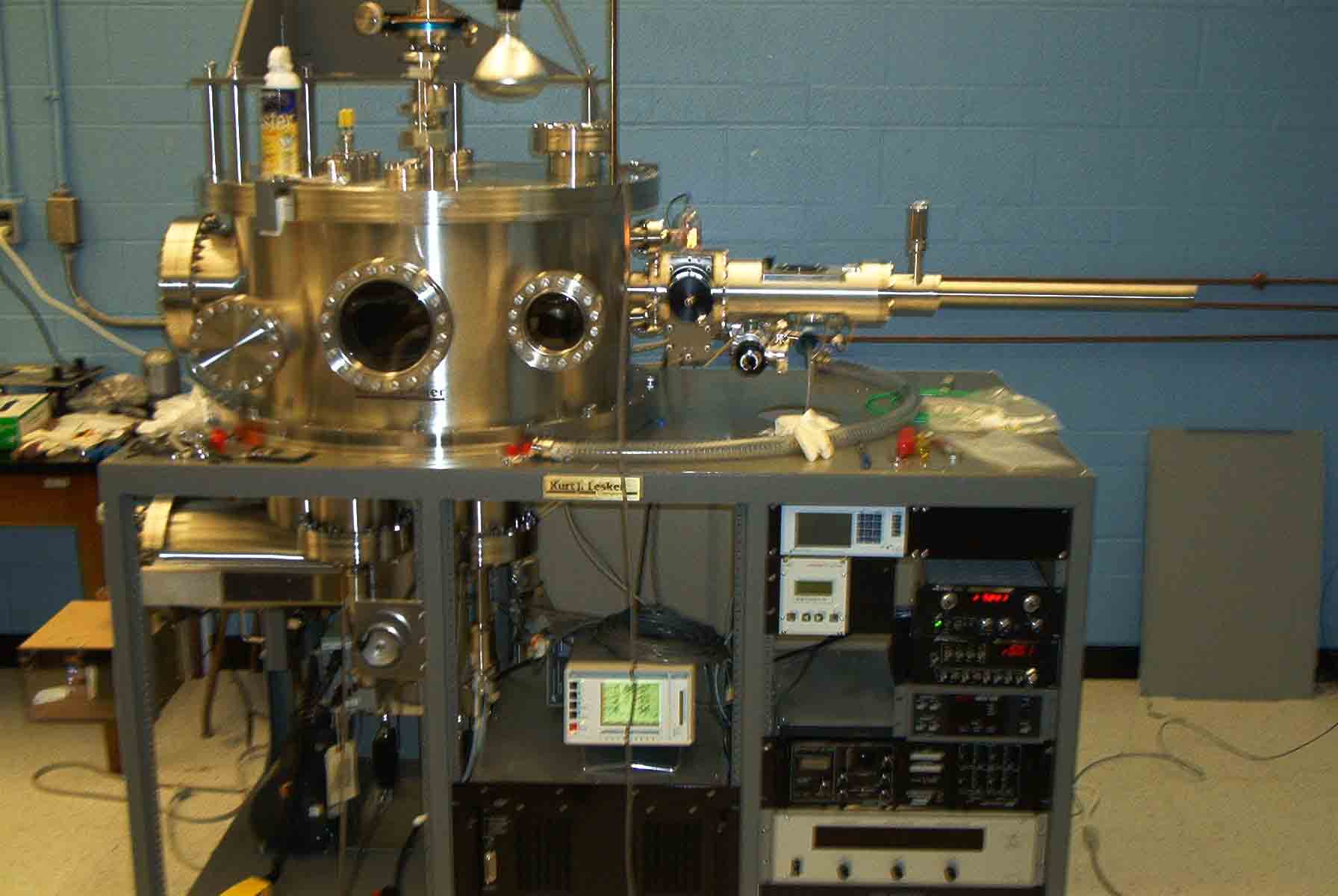
A
multiple-purpose vacuum chamber, supplied by Kurt Lesker Co., is
dedicated to materials processing of thin-film samples. The
chamber is completely bakeable and equipped with a large-volume
turbomolecular pump to achieve ~10-7Torr base pressure.
Multiple port design enables a variety of processes (see below), with
the sample holder on a 4-stage carousel, with both button-heating and
liquid-nitrogen cooling capabilities. A load-lock hatch enables
quick sample transfer.
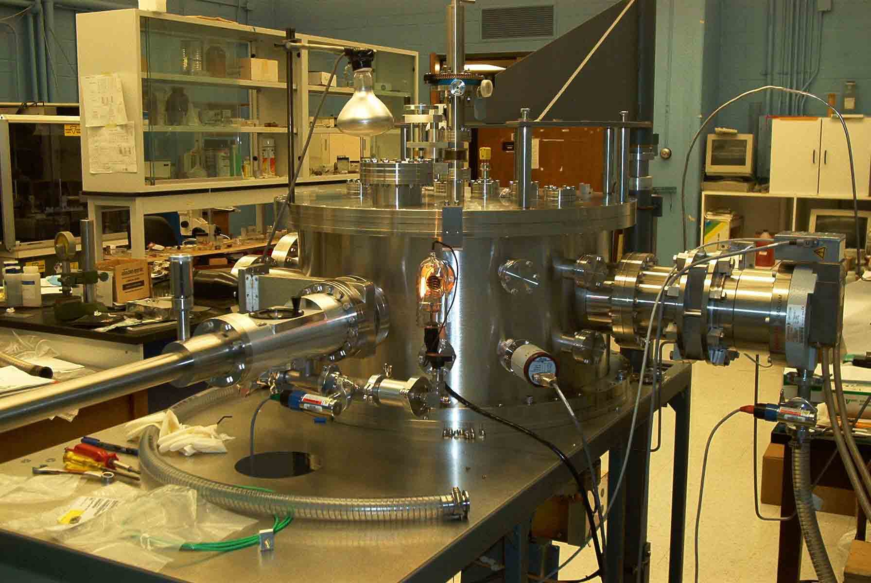
This vacuum
chamber is equipped for a variety of processes. First, there are
DC and RF sputtering guns for thin-film deposition from 2-inch targets
of both non-magnetic and magnetic materials. An extractable
vibrating-quartz head can be used to monitor the film thickness during
deposition. Second, there is an ion-milling gun for physical
etching of pattern-masked thin films. The ion milling can be
carried out with the sample holder cooled by liquid nitrogen, to protect the
sample from ion damage, which is particularly detrimental to complex
oxide materials. Third, there is a thermal evaporator for
deposition of stock materials. In addition, there is an
electron-gun evaporator, with rasterable beam and multiple pockets, to
enable the deposition of materials requiring higher energies.