PHY405 Electronics, Lab 3
Adapted from Prof. David Bailey's website in 2022
Overview
- RLC resonant circuits
- Diodes
- Design AC to DC Converter
Background preparation before starting the lab
- Read through all these Lab instructions before the lecture.
- Before the lab, do anything (e.g. design, analyze, read, watch, …) that can be done before the lab.
- Especially try to design the two circuits before the lab!
Safety
When applying voltages across resistors, remember that \(P=V^2/R\).
- If something starts to smoke, turn off the wave generator or DC power supply.
- When changing a component, be cautious in case it is hot.
- NEVER LEAVE YOUR CIRCUIT UNATTENDED WITH THE POWER ON!!!
Exercises
LCR Resonant Circuit
Design and build a circuit with a resistor, capacitor, and inductor in series with the wave generator, such that the Output taken across the resistor has
- a resonant peak of \(7\pm1\) kHz.
- the highest possible Quality (Q) factor given the components available to you.
- attenuation at the peak not more than 4db.
- In an ideal circuit with an ideal wave generator this would be 0db.
Study the attenuation and phase vs frequency characteristics of the circuit.
Include in your report:
R-1) A Falstad simulator circuit simulation screenshot or other circuit diagram. Be sure the component values are all clearly visible.
R-2) A photo of the actual circuit.
R-3) A Bode plot of the attenuation/Magnitude and phase of the Output signal, over a frequency range from 10Hz to 20MHz, with the output taken across the resistor.
For the Bode plot,use the scope’s Frequency Reponse Analysis (FRA) function, either directly or remotely via USB control.
- The FRA display data can be downloads via the Front USB port onto a memory skey
- Insert memory key into front USB port.
- Press Save/Recall button. then
- Save
- Select Format as Frequency Response Analysis data (\(\ast\).csv) -Save To should show USB key
- Save to USB
R-4) Is the spectrum consistent with expectations from the simulation? If not, modify your Falstad simulation so that it roughly agrees with what you see. Include a screen shot of the modified circuit simulation.
- Some common issues.
- A real power source has an internal resistance.
- Real inductors have series resistance, parallel self-capacitance, and parallel resistance. The latter can probably be ignored, but the first two can be measured with your multimeter.
- The non-ideal characteristics of real capacitors are even more complicated, but can probably be ignored here.
R-5) Include in your report a Bode plot showing the attenuation/Magnitude and phase of the Output signal, over a frequency range from 10Hz to 20MHz, with the output taken across the inductor+capacitor.
- If what you see doesn’t make sense, you may not have thought about your ground connections.
- This arrangement acts as a notch filter that could be used to reduce an unwanted background 7 kHz component in a signal. A larger value for R would increase the attenuation at 7 kHZ, but decrease the frequency selectivity.
I-V Characteristics of a Diode
Diodes are not linear devices. The current (I) through them is not simply proportional to voltage (V), and they preferentially allow current to flow in the forward direction, but not in the backward direction.
- Use the same type of blue that you used previously in Lab 1.
- Put the LED in series with your multimeter and your DC power supply Output 1.
- Set the current limit to 0.1A!! (This is already 5x the rated current for the LED, and going higher will destroy the LED.)
- Initially set the voltage to 3V to make sure the LED lights up, if not, it probably just needs to be reversed.
- Measure the current with your multimeter.
The effective reverse resistance is not infinite, but we will not try to measure it since this is difficult with the breadboard set-up.
Diode I-V Model
The simplest model for the forward current of a real p-n junction diode is that it grows roughly exponentially
\[i = i_s\left(e^\frac{eV}{k_BT} - 1\right)\]
where \(e\) is the electron charge, \(V\) is the voltage across the diode, \(k_B\) is the Boltzmann constant, \(T\) is the diode temperature, \(i_s\) is the reverse bias saturation current.
R-6) Is the I-V curve of the blue LED in the forward direction roughly consistent the above exponential model?
- A fit is not necessary. Just see if \(I\) vs \(V_{LED}\) in the forward direction is roughly linear on a semilog plot.
Zener Diode
A quick but less precise why to indirectly see the I-V characteristics of a diode is put the diode in series with a resistor, apply a ramp voltage, and use your oscilloscope in X-Y mode.
- Disconnect the DC power supply and multimeter from your circuit.
- Connect the Wave Gen across the diode and a 1k resistor in series, and monitor the Wave Gen voltage with scope Channel 1.
- Connect Channel 2 across the resistor.
- Set the Wave Generator* to
- Waveform \(\rightarrow\) Ramp
- Frequency \(\rightarrow\) 50Hz
- Amplitude \(\rightarrow\) 20Vpp
- Adjust Horizontal settings so you have a few cycles on screen.
- press Acquire, then set
- Time Mode \(\rightarrow\) XY
- Acq Mode \(\rightarrow\) High Res
- Tweak Channel 1 & 2 settings so display fills (but does not overflow) screen.
Channel 2 shows the voltage across the resistor is proportional to the current flowing through the circuit, since \(I=V/R\). The voltage across the diode can be calculated from \(V_{LED}=V_{in}-V_R\), so the display tells us about the I-V characteristics of the diode. You should see something like this:
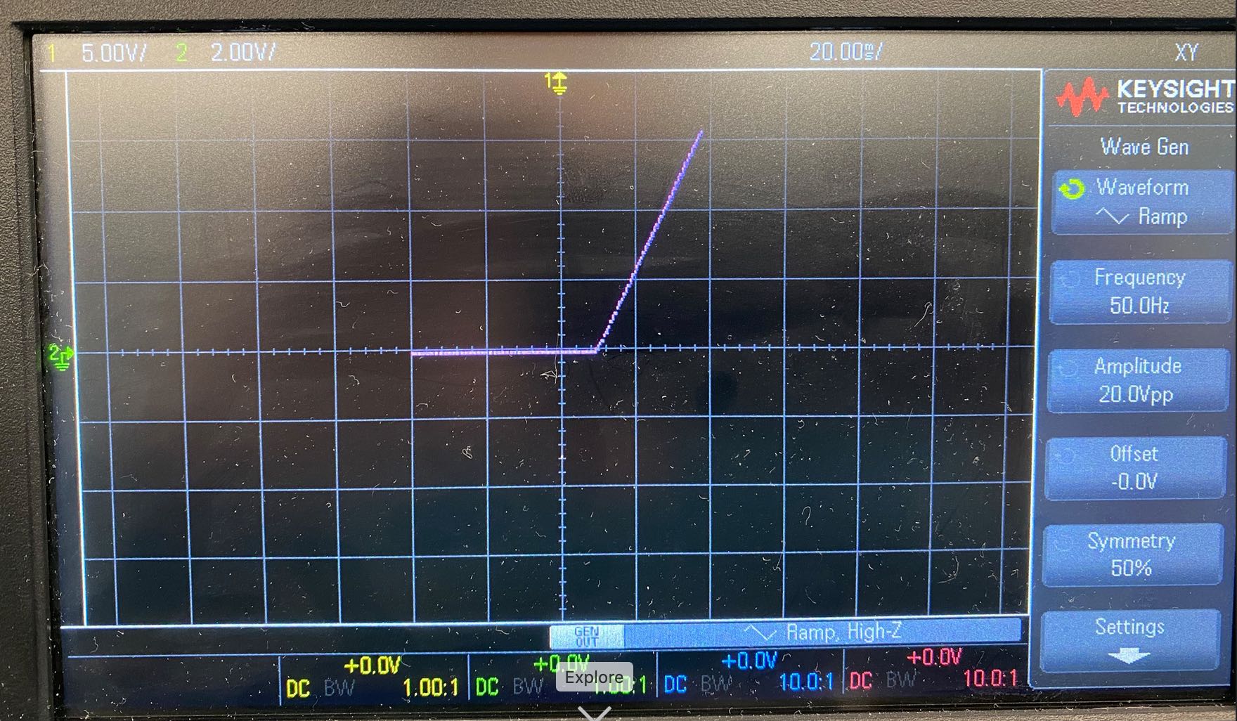
\(V_R\) vs \(V_{in}\) for blue LED in series with a 1k resistor. When current is flowing in the forward direction (on the right), the LED has almost zero effective resistance so all the voltage drop is across the resistor and is proportional to the applied voltage. When the current flows in the diodes backward direction, the diode has extremely high effective resistance so almost all the voltage drops across the diode and almost none across the resistor - hence the flat line on the left.
Replace the blue LED with a nominal 3.9V zener diode. At high enough reverse voltage, all diodes eventually break down and conduct, but zener diodes have relatively low and well defined breakdown voltages that can be used to limit and control voltages in a circuit.
R-7) Include a photo of the display for the zener diode and qualitatively explain what you see.
AC-to-DC Power Supply
A basic, albeit not very efficient, AC to DC converter can be created by simply inserting a diode to rectifyat the input of an RC Low-Pass filter. The diode rectifies the voltage, allowing the capacitor to charge when current is flowing though the diode in the forward direction, but preventing the capacitor from discharging when the voltage is reversed. As long as the RC time constant is much longer than the AC input frequency, the capacitor will charge to close to the peak AC voltage. A zener diode can be put across the output for a fixed output voltage lower than the peak AC voltage.
- The RC time constant should be much longer than the AC input frequency.
- An electrolytic capacitor is fine, but make sure it is inserted with the correct polarization.
- When simulating this, some additional resistors may be needed to prevent shorts.
R-8) Using a 1N4001 rectifier diode, a 3.9V zener, a capacitor, and whatever resistor(s) you need, design and build an circuit that takes a 20Vpp 60Hz square-wave input and outputs about 3.9V DC across a 1k output resistor, with less than about 5% ripple.
- Any DC voltage in the range 3-5V is fine.
- The 1k resistor is the output load; it is not the R in the RC circuit.
- Ripple is the amount of AC variation in the output.
Include in your report a Falstad circuit simulation of your final design, and include a photo of your scope showing the AC input and DC output signals.
Clean-up
- Properly dispose of any waste, e.g. wire cuttings or insulator cuttings
- But keep any small connector wires you may have made, they will be useful over the semester.
- If a component has been damaged, e.g. it smoked because of overheating, dispose of it.
- Turn off all equipment.
See you next week!