PHY405 Electronics, Lab 4
Adapted from Prof. David Bailey's website in 2022
Overview
Operational amplifier fundamentals and examples:
- Open Loop, Non-inverting, Inverting, Input impedances, Design challenges
Background preparation before starting the lab
- Read through all these Lab instructions before the lecture.
- Before the lab, do anything (e.g. design, analyze, read, watch, …) that can be done before the lab, e.g.
- Exercises R-7 & 8 are not done in the lab, and are best done before the lab.
- The design for exercise R-9 should be done before the lab.
Safety Reminders
Active components, especially some transistors and op-amps, are much more sensitive to static electricity than passive components such as resistors, inductors, and capacitors. BE CAREFUL!!
- Static discharges can destroy equipment and component. You are especially likely to zap your circuit if
- you wear synthetic clothing
- sit on a plastic chair with plastic wheels that rolls on a carpet (like MP257)
- Always discharge yourself before touching any components.
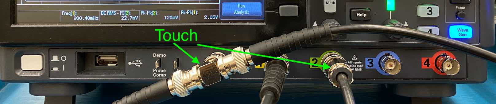
You can discharge yourself by touching this grounded scope connections
Operational amplifier
An operational amplifier (“op-amp”) is one of the most important active components in electronic circuits.
An ideal op-amp has infinite gain when the output is not connected to the input, and real op-amps typically have such “open loop” gains of \(10^5-10^6\). An ideal op-amp has zero output impedance so its output voltage is independent of the output current. The “golden rules” for an ideal op-amp are:
- It has infinite input impedance so the inputs draw no current.
- In a closed loop with feedback, the output adjusts itself to make the voltage difference between the inputs zero.
Exercises
Insert an LF356 op-amp into the breadboard.
- The gap in the middle of each breadboard is designed so standard integrated circuits fit.
- Be careful to align the pins with the holes. If you force in a misaligned pin you can break it.
- If the pins are splayed, you can very gently try to straighten them with your pliers.
Use the power supply to create positive and negative supply rails (V+ and V-) on your breadboard to power the op-amp.
- The power supply has a tracking button, that you can press and hold to set the Outputs \(2\) (green) and \(3\) (blue) to be equal in magnitude (but opposite in sign).
- Set the supply for a symmetric +15 V output from the green terminal and -15V from the blue terminal.
When you make your circuit, the common ground is established by the connections to your oscilloscope and function generator
- Connect the DC power supply COM terminal to your breadboard ground.
- Use hookup wire to connect the ground for your circuit to your breadboard ground.
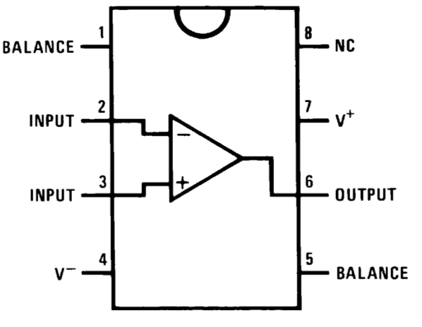
Pin assignments for the LF356 chip from its datasheet.
Open Loop Characteristics
An op-amp in open loop mode is inherently unstable and has relatively narrow bandwidth compared to the circuits with feed-back you will build later.
- The output voltage of an op-amp cannot lie outside the range of its DC power supply voltages
- Too large an AC input into a high gain amplifier will make the output “rail”, i.e., hit the limits on its output and get clipped.
- e.g. an op amp powered from ±15 V cannot produce an AC output with peak-to-peak voltage greater than 30V.
- Too large an AC input into a high gain amplifier will make the output “rail”, i.e., hit the limits on its output and get clipped.
- Given their huge open loop gain, even tiny amounts of noise leaking into an op amp can have large effects on their output.
- Always use decoupling/bypass capacitors at the power supply pins of each op-amp in every circuit to prevent high frequency noise leaking into the op-amp output. Most schematics do not explicitly indicate these capacitors (or even the power connections), but you should always use them; \(\sim 0.1-1 \mathrm{\mu F}\) are reasonable values. (see Figure 1)
Create the circuit in the figure below with a LF356 op amp and \(\sim 0.1-1 \mathrm{\mu F}\) decoupling capacitors.
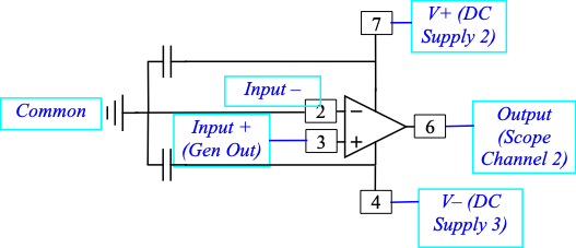
Open loop op amp circuit. Note the decoupling capacitors from the DC power inputs to Common.
To help ensure correct wiring, it is recommended that you always use the same colour. For example
- Any black wire is connected to Common.
- Any green wire is connected to V+ (DC Power Supply Output 2).
- Any blue wire is connected to V— (DC Power Supply Output 3).
- Any red wire is an Input or Output
- Power with the ±15 volt tracking outputs from your DC supply.
- I recommend using the Wav Gen option (instead of Channel 1) for the Trigger.
R-1) Provide a scope screen image of the op am Output for a 10 Hz 10 mV amplitude Ramp wave Input.
R-2) Explain what you observe.
- If needed, unclicking the Supplies Tracking box and changing the DC supply voltages independently, and playing with the WaveGen signal parameters may help your understanding.
Op amps With Feedback
Feedback is the process where the output of a system is used as input to control and modify the system. All commonly useful op amp circuits depend on feedback.
Non-inverting amplifier
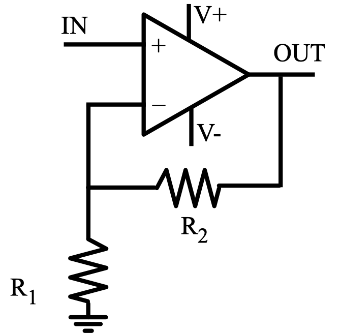
A non-inverting amplifier with output voltage \(V_{out} = \left(1 + \frac{R_2}{R_1}\right)V_{in}\). The DC power decoupling capacitors are not shown, but they still must exist.
Create feedback for your Op Amp by connecting the inverting input (-) to a resistive voltage divider acting on the output, as shown above. Select the two resistors \(R_1\) and \(R_2\) to give a gain of \(\sim 100\).
- The decoupling capacitors are not shown, but they still must exist.
- Be careful. It is easy to:
- Make incorrect connections, e.g. insert a wire into the wrong row.
- Create unintentional connections, e.g. when two resistor leads in different rows accidentally touch.
R-3 What resistance values and tolerances did you choose for \(R_1\) and \(R_2\)?
R-4) Measure the amplifier’s transfer function (\[ H(f) = \frac{V_{Output}(f)}{V_{Input}(f)}\] for sine wave signals between 50 Hz and 5 MHz. Does it agree with what you expect?
- To avoid exceeding the scope’s input voltage, in FRA Setup, set the Amplitude to 100 mVpp.
R-5) Are the observed maximum gain and observed bandwith what you expect?
- The expected (i.e. typical) Gain \(\times\) Bandwidth is available from the op amp’s spreadsheet.
- The bandwidth of a low-pass filter is the frequency of the 3db point.
Inverting amplifier
The previous non-inverting amplifier cannot have a gain less than 1, but an inverting amplifier can.
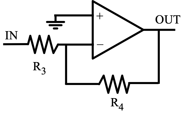
An inverting amplifier with output voltage \(V_{out} = -\frac{R_4}{R_3} V_{in}\). Note that this diagram follows the common convention that the DC power connections are not shown, but they obviously still exist.
Construct an inverting amplifier as shown in the above figure, choosing \(R_3\) and \(R_4\) to give a gain of \(\sim 100\).
R-6) Provide a scope screen image showing that the amplifier does invert the input signal.
- An inverted sine wave could just be 180° out-of-phase, so a pulse Wav Gen output is better to show that it is inverting.
Input impedance
One of the most important difference between non-inverting and inverting op-am circuits is their very different input impedances.
Input impedance is simply the ratio of input voltage to input current, i.e. \(Z_{in}=|V_{in}|/|I_{in}|\). An amplifier with very large input impedance is insensitive to the impedance of whatever input circuit is providing the input signal to the amplifier. (Here the input circuit is the wave generator and associated connections.) Since the amplifier input impedance is the load impedance for the input circuit, \(|Z_{in}|\) must be large enough so that the input circuit signal is not degraded because the the input circuit cannot provide enough power (\(P_{in}=V_{in}^2/|Z_{in}|\)).
It can be hard to directly measure the input impedance of a high gain op amp circuit, so we will use simulations to get a feeling for the different impedances of op amp circuits.
- Instead of assuming an ideal op amp, the “real” simulations are based on a LM741 op amp.
- \(V_{in}\) and \(I_{in}\) in these circuits are simply the voltage and current of the AC supply.
R-7) What are the input impedances of each of these circuits?
A) ideal non-inverting amplifier (Click on link to see Falstad circuit)
B) “real” non-inverting amplifier
R-8) What changes would you make to the resistor valuesin order to double the input impedance while keeping the same gain for the following circuits
A) A “real” inverting amplifier circuit
B) A “real” non-inverting amplifier
If it is not possible, say so.
Design tasks
More complex op amps have many capabilities. For example, here is a summing amplifier Falstad circuit that allows you to scale and add signals. (There is also a Falstad example.)
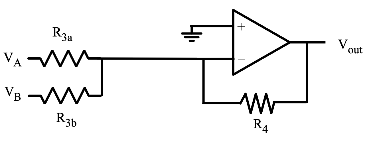
An inverting summing amplifier with output voltage \(V_{out} = -\frac{R_4}{R_{3}a} V_A - \frac{R_4}{R_{3b}} V_B\).
R-9) Complete either one of the following tasks A or B. Include in your report:
- a circuit diagram or Falstad simulation screen-capture that clearly shows the circuit and all the component values.
- a photo of your working circuit.
- a scope screen image showing that the circuit does what it is expected to.
If you do both, you can get extra credit (but your final mark for the exercise cannot exceed 10/10).
Remember to check out the Falstad circuit examples, in case they have something close to what you want.
A) Using a single op-amp and some resistors, design and test a differential amplifier circuit whose output is equal to about 1.8 times the difference \(V_A-V_B\) between two arbitrary (within reason) input voltages, \(V_A\) and \(V_B\).
- Use the Demo Probe Comp signal (~1kHz square wave, ~2.5Vpp) as \(V_A\) and a Wav Gen signal for \(V_B\).
- You can use an alligator clip to connect to Demo Probe Comp
B) Design and test an amplifying bandpass filter circuit that will amplify signals between very roughly 400Hz and 9kHz by a factor of 100, but attenuates any signals outside this band. You can only use a single op-amp, but multiple resistors or capacitors.
- The range is very rough, e.g. anywhere in the range 300-500 Hz for the low cutoff, 5-15 kHz for the high cutoff, and 75-150 in gain is fine.
- Pay careful attention to the loading of filter sections by the input impedance of the amplifiers. The order of filters matters.
- We only care about the amplitude, i.e. it doesn’t matter if the output is inverted or not.
- If the bandpass or gain isn’t as expected, one can change the capacitors and resistors to improve the circuit.
End of Lab
Clean-up
- Properly dispose of any waste, e.g. wire or insulator cuttings
- But keep any small connector wires you may have made, they will be useful over the semester.
- If a component has been damaged, e.g. it smoked because of overheating, dispose it.
- Turn off all equipment.
See you next week!