
Alan Stummer, Research Lab Technologist
Coincidence Detector
Downloads
Revision Overview
System Overview
Hardware
Firmware
Software & Protocols
Simple GUI
Downloads
- All files
- Schematic and PCB (Eagle), also schematic in PDF (may not be the latest)
- Verilog source code and Quartus II project.
- Simple GUI source code (VB)
NOTICE: This webpage and associated files is provided for reference only. This is not a kit site! It is a collection of my work here at the University of Toronto in the Physics department. If you are considering using any schematics, designs, or anything else from here then be warned that you had better know something of what you are about to do. No design is guaranteed in any way, including workable schematic, board layout, HDL code, embedded software, user software, component selection, documentation, webpages, or anything.
All that said, if it says here it works then for me it worked. To make the project work may have involved undocumented additions, changes, deletions, tweaks, tunings, alterations, modifications, adjustments, waving of a wand while wearing a pointy black hat, appeals to electron deities and just plain doing whatever it takes to make the project work.
Revision Overview
Initial release of hardware, firmware and test software is as described below. The Verilog has been archived and superceded as follows.In April 2007, I revised the hardware to Rev:C and Jeff Lundeen et al (Ultrafast Quantum Optics Group, Clarendon Laboratory, Department of Physics, University of Oxford) reworked the Verilog. They changed the coincidence detection from the original laser clock based to FPGA register based. I subsequently revised that for Krister's board (4 APDs, System Verilog, more comments, minor editorial) and loaded that new firmware. This version varies from the following description in that the modus operandi is as just described but otherwise remains as before and fully back compatible.
System Overview
The purpose of the coincident detector is to detect simultaneous pulses between four to six APDs Avalanche PhotoDiodes). Specifically, a laser pulse may cause a photon to appear at any one, two or up to six of the APDs. The area of interest is when two or more APDs detect photons from the same laser pulse. Specs and functional definitions include:
- 4 or 6 APD inputs on BNC connectors.
- APDs are 25nS TTL compatible pulses, +4.5V into 50Ω with 2nS rise and fall times, 0V off. APDs take about 50nS to reset after end of pulse before start of next possible pulse.
- Laser input is from fast unamplified photodiode, automatic tracking of slice level to maintain 50% duty cycle.
- Coincidence defined as overlapping of beginning of two pulses. Valid coincidence < 2nS ±0.5nS.
- Each possible combination of coincidence counted separately with array of 40-bit counters for all permutations of APDs.
- Pulse repetition rate (AKA pulse period) 12.5nS (80MHz), possibly down to 10nS (100MHz) in future.
- Computer interface by USB for reading of counters and control of counters and byte serializer.
- Computer sets number of laser pulses in 40-bit counter, data logging during that period only.
- During computer communications, data logging is halted.
- Altera FPGA used as much as possible to reduce hardware. Verilog language. Altera Cyclone series in a QFP.
- Signal phasing to be externally adjusted to <2nS by varying lengths of cables. APDs all to be in same phase, laser phase adjusted relative to APDs phase for proper clocking. Correct phasing to be determined empirically by finding minimum and maximum cable lengths which work then setting length to between them.
Hardware
Refer to the schematic (in its native Eagle format, but may be newer than this description), or in PDF.
FPGA The circuit has an Altera Cyclone EP1C12Q240C6 battleship with some support circuits. The FPGA core is +1.5V, the I/Os are +3.3V. It uses a standard EPCS4 serial configuration IC. Normal programming is via the Active Serial ("AS") port to the configuration IC, or a volatile SRAM programming via the JTAG port. Boundary scan is not done. The IC2 POOR IC is not used but is available for DEV_CLRn if required for future use. The same applies to R17 on pin 239 DEV_OE and the crystal oscillator IC3 on pin 28 CLK0.
Power Supply The power supply consists of two Lidos in series. First, IC8 drops the incoming +5V to +3.3V for the I/Os, then IC9 drops the +3.3V to +1.5V for the core. Virtually all of the power is consumed by the core, so the power dissipation is split between the two regulators. Although the maximum inrush to the FPGA can be as high as 900mA, the Lidos' current limiting has a slight delay and will allow the FPGA to start. The incoming +5V supply calculates to 200mA maximum but is observed at under 100mA at 80MHz. It can be provided by a small regulated adaptor or simply taken from the USB bus. The latter is recommended.
USB Interface The USB interface IC10 is done with a single IC from Delcom, based on the Cypress CY7C63001. It features USB1.0 to two 8-bit ports and comes preprogrammed for parallel, SPI, I 2C and serial protocols. This chip saves a lot of work and is worth many times its selling price in saved development time in low volume applications. Drawing its +5V supply from the USB bus, two resistors and a 6MHz crystal make a complete interface. The ports have open drains with resistive pullups. It is configured as Port0 being an output (FPGA operating mode) and Port1 as a bi-directional data bus. To avoid bus contention on Port1 (in case of reprogramming and there is contention), 1K resistors have been added to each bit so that the FPGA dominates and nothing is harmed. Bits P0.6 and P0.7 are active low LEDs, or any other 5V. These LEDs can be activated by either the FPGA or the USB, however the former is discouraged due to the possibility of bus contention.
The USB interface IC does not have an explicit tri-state mode. Because of the active pulldowns and passive pullups, outputting 0xFF effectively turns the port into either an output with all bits high or an input where the FPGA overrides the relatively weak passive pullups. Therefore to read Port1, output 0xFF to release it then read it back. The FPGA has explicit data bus tri-state controls as described below.
Laser Slicer The pulse laser input is from a photodiode, giving Gaussian shaped pulses of about 200mVp over 2nS. The comparator IC5 slices it into LVPECL outputs. They go to the LVPECL to TTL level shifter IC7, the output of which goes to an input on the FPGA. The complimentary LVPECL lines are low passed filtered and fed into the relatively low speed opamp IC6. This opamp keeps the two LVPECL lines at the same average voltage by adjusting the laser slice threshold, therefore not only adapting to a wide range of input levels and offsets but maintaining a 50% duty cycle to the benefit of the Fog's clock bus.
APD Inputs Last but not least are the TTL inputs from the APDs. The 50 Ohm terminations provide transmission line termination, while the two divider resistors convert the levels to LVTTL.
Firmware
The firmware code is in Verilog.2001 using Altera's Quartus II V4.1. There are two user selectable parameters. First, select the number of APDs; 2 for testing and development, 4 or 6 for operation. Second, set the 5-bit revision number. This is a simple count used by the computer to confirm that the minimum firmware revision is in use. The final revision number sent is with the 3 MS bits set for the number of APDs and the 5 LB bits as this revision parameter.
Operation Mode Control All operation of the FPGA is controlled by the operation mode as given by the state of the USBctrl bus, the Port0 from the USB device. The operation mode is level sensitive, it is checked on the rising edge of every laser pulse. There are ten valid operation modes, all others are ignored and harmless. IMPORTANT : The laser must be running for any communications with the FPGA! This is because the firmware is all clocked by the laser so that the maximum laser clock speeds are possible.
Combinational Logic & Registers The bi-directional bus control and the APDs concatenation are done in combinational logic, the former because it has to be real-time to prevent bus contention and the latter so that the six APDs can be converted into binary weighted bits in a single APD byte. An array of 40-bit unsigned integer counters is used to count the coincidences. There is one counter for each possible combination of APDs plus one for the laser. Therefore, for 4 APDs there will be 2 4 + 1 or 17 counters, for 6 APDs there will be 2 6 + 1 or 65 counters. The counters are numbered by the binary value of the concatenated APDs. For example, no APDs on is counted by Counter[0], APD-A only is counted by Counter[1], APD-A and APD-B both on is counted by Counter[3], etc. The laser count is held by Counter[16] for 4 APDs or [64] for 6 APDs.
"Always" Loop The remainder of the Verilog is in a single "always" loop, triggered on the rising edge of the laser. Execution then depends totally upon the command mode set by USBctrl, the USB interface's Port0 output. The 4 LS bits determine one of ten modes, including presetting the laser counter, counting coincidences, resetting the read state machine, reading the counters and reading the firmware revision. All operation modes are enabled by bit 4 of USBctrl. Because the modes cannot be in Grey code, bit 4 has to be set false before changing modes. Specifically, the asynchronous and relatively slow USB Port0 may transition many possible operation modes while its output logic levels slew and the high speed FPGA would interpret all of the intermediaries. The safe protocol is given below.
Prevention of Multiple Counts Because the APDs stay on for several laser pulses after being tripped, only
the first occurrence can be counted. The two lines after the "always" statement handle that.
*
APDs_New <= APDs & APDs_Old;
This line will flag any APD which has yet to be counted.
*
APDs_Old <= ~APDs;
This line will nflag any APD which is to be ignored.
However, if an APD fires while another APD has yet to reset itself, the latter will be ignored. For example,
if APD-A fires then it will be counted as a single event on Counter[1]. If on the next laser pulse APD-B fires
and APD-A will still be fired, then only APD-B will be counted, on Counter[2]. This is unavoidable, it is the
nature of the APDs.
Count Mode The count mode, the raison d'être of this whole contraption, serves two functions. It increments one of the array of counters, depending on the concatenated APDs. In practice, most of the time there will be no APDs on so the "none" counter is incremented. Similarly, Counter[15] (for 4 APDs or [63] for 6 APDs) is rarely incremented because that would involve all APDs firing at the same time. The other function of the count mode is to keep track of the number of laser pulses and then to stop counting when finished. This is done by decrementing the laser counter, which has been preset to the number of experiments to be run. As long as the laser counter is above zero, coincidence counting is allowed and a flag is set on USBdata.0 to show the USB and computer that the experiments are still running. Once the required number of experiments has been run and the laser counter reaches zero, the USBdata.0 flag is cleared and all further laser pulses are ignored while in count mode.
Counter Reset Mode The counter reset mode simply resets all counters to zero, including the laser counter. This mode only has to be entered to take effect.
Laser Preset Mode There are five laser preset modes, one for each of the five laser counter bytes. Entering a laser preset mode will copy the USBdata byte into the appropriate laser counter byte. All five bytes must be set if the counter is to be definitive. This 40-bit count says how many experiments to run before stopping, up to a maximum of 2 40 or about 10 12 or about 3.8 hours at 80MHz. This count will be decremented by on each laser pulse. Note that the number of experiments can be extended past 2 40 times by presetting the laser again once the experiments end without resetting the counters, however, some counters may overflow.
Read Reset Mode The read reset mode will initiate the read state machine by pointing at the first (LS) byte of the first counter, Counter[0], in preparation to reading the counters. This mode only has to be entered to take effect.
Read Counters Mode The read counters mode presents each byte of each counter sequentially to the USB interface. It must be preceded by the read reset mode. The bytes are read back one at a time starting with the first (LS) byte of the first counter, Counter[0]. Each subsequent entry to the read counters mode will present the next byte. For example, following a read reset mode, the first byte presented in the read mode is Counter[0][7:0]. The next read counter mode will present Counter[0][15:8], the next is Counter[0][23:16], then Counter[0][31:24], Counter[0][39:32], then the next counter Counter[1][7:0], Counter[1]15:8], etc. This continues byte by byte, counter by counter, until finally the laser counter is done. For 4 APDs, there are 5*(2 4+1) or 85 read modes required, for 6 APDs there are 5*(2 6+1) or 325 read modes required. The read counters mode is non-destructive. At any time the count can be stopped, the counters read and then the count resumed. Note that for a completed run of experiments the laser counter will be zero, although a non-zero count is harmless and means that the run was manually terminated or paused.
The pointer to the next byte to be read is incremented after the read counter mode is exited and any invalid mode is entered.
Read Firmware Revision Mode The read firmware revision mode presents the firmware revision byte (including the number of APDs) to the USB interface. This allows the computer to verify that a valid firmware revision is running and how many APDs it was compiled for.
Software & Protocols
The operating mode is set by the five LS bits of the USB's Port0. The operation mode is level sensitive (the actual mode is the present state of Port0 at all times). As stated above, Port0.6 and Port0.7 are used for the LEDs and do not affect the operating mode. Port0.5 is unused, its state is irrelevant at all times.
| USBctrl |
Mode |
Description |
| xxx10000, 0x10 | Preset Laser 0 | USB writes to the laser counter, LS byte. |
| xxx10001, 0x11 | Preset Laser 1 | USB writes to the laser counter. |
| xxx10010, 0x12 | Preset Laser 2 | USB writes to the laser counter. |
| xxx10011, 0x13 | Preset Laser 3 | USB writes to the laser counter. |
| xxx10100, 0x14 | Preset Laser 4 | USB writes to the laser counter, MS byte. |
| xxx10101, 0x15 | Reset Counters | All counters are set to zero. |
| xxx10101, 0x16 | Count | Experiment runs, coincidences counted. |
| xxx10101, 0x17 | Read Reset | Prepare to read the counters. |
| xxx10101, 0x18 | Read Counters | Read the next byte in the counter array. |
| xxx10101, 0x19 | Read Firmware Revision | Read the firmware revision byte. |
USB Device Refer to the Delcom manual for further details. Install the windows driver. The driver may have to be moved to a windows system directory if windows cannot find it. Use the variable structures, DLLs and examples given by Delcom. Only two USB commands are required: write to both ports and read from both ports. Optionally, the USB's UDSN (Unique Device Serial Number) and firmware version may be read to identify the hardware. To write to the ports, set the port values, major & minor commands and call the write function. Reading is similar except that the port values are in the first two bytes of the function's return structure.
Changing Operating Modes Each operating mode has three stages: setup, execute and exit. During all three stages, the four LS bits must remain static and only Port0.4 can toggle. To setup an operating mode, keep bit 4 low and set bits 0 to 3 to the required operating mode. Set bit 4 high to enter the operating mode. Maintain this as long as required, although most modes are not time sensitive and can be pulsed or held (only count mode requires the mode to be held until counting is finished). Finally, set bit 4 low to disable the operating mode. It is now safe to setup for the next operating mode.
The only exception to this 3-step rule is when reading the counters. Because the setup and exit commands, 0x08, are the same and sequential, they become redundant. Only one is needed.
Example Sequence For example, the following is a complete sequence for running 10 6 experiments (where "read" means to read Port1). The LEDs are assumed to be off, although to turn on an LED any command can be logically AND'd with 0x7F to turn on LED1 and/or with 0xBF to turn on LED2, or OR'd with 0xC0 to turn them both off.
| Step | Port0 | Port1 | Description |
| 1 | 0x05 | 0xFF | |
| 2 | 0x15 | 0xFF | Reset counters |
| 3 | 0x05 | 0xFF | |
| 4 |
0x00 |
0x40 | |
| 5 | 0x10 | 0x40 | Preset laser counter, LS byte. |
| 6 | 0x00 | 0x40 | |
| 7 | 0x01 | 0x42 | |
| 8 | 0x11 | 0x42 | Preset next laser counter byte. |
| 9 | 0x01 | 0x42 | |
| 10 | 0x02 | 0x0F | |
| 11 | 0x12 | 0x0F | Preset next laser counter byte. |
| 12 | 0x02 | 0x0F | |
| 13 | 0x03 | 0x00 | |
| 14 | 0x13 | 0x00 | Preset next laser counter byte. |
| 15 | 0x03 | 0x00 | |
| 16 | 0x04 | 0x00 | |
| 17 | 0x14 | 0x00 | Preset laser counter, MS byte. |
| 18 | 0x04 | 0x00 | |
| 19 | 0x06 | 0xFF | |
| 20 | 0x16 | 0xFF | Count coincidences |
| 21 | 0x16 | read | Read ports |
|
The experiments are running. Repeat step 21 over and over until Port1.0 is low, indicating that the experiments have finished, or, stop the run early by jumping to step 22. |
|||
| 22 | 0x06 | 0xFF | Exit count mode |
| 23 | 0x07 | 0xFF | |
| 24 | 0x17 | 0xFF | Read reset |
| 25 | 0x07 | 0xFF | |
| 26 | 0x08 | 0xFF | |
| 27 | 0x18 | read | Read Counter[0], LS byte |
| 28 | 0x08 | 0xFF | |
| 29 | 0x18 | read | Read Counter[0], next byte |
| 30 | 0x08 | 0xFF | |
| 31 | 0x18 | read | Read Counter[0], next byte |
| 32 | 0x08 | 0xFF | |
| 33 | 0x18 | read | Read Counter[0], next byte |
| 34 | 0x08 | 0xFF | |
| 35 | 0x18 | read | Read Counter[0], MS byte |
| 36 | 0x08 | 0xFF | |
| 37 | 0x18 | read | Read Counter[1], LS byte |
| 38 | 0x08 | 0xFF | |
| 39 | 0x18 | read | Read Counter[1], next byte |
| 40 | 0x08 | 0xFF | |
|
Repeat until... (4 APDs shown) |
|||
| 183 | 0x18 | read | Read Counter[15], next byte |
| 184 | 0x08 | 0xFF | |
| 185 | 0x18 | read | Read Counter[15], MS byte |
| 186 | 0x08 | 0xFF | |
| 187 | 0x18 | read | Read Counter[Laser], LS byte |
| 188 | 0x08 | 0xFF | |
| 189 | 0x18 | read | Read Counter[Laser], next byte |
| 190 | 0x08 | 0xFF | |
| 191 | 0x18 | read | Read Counter[Laser], next byte |
| 192 | 0x08 | 0xFF | |
| 193 | 0x18 | read | Read Counter[Laser], next byte |
| 194 | 0x08 | 0xFF | |
| 195 | 0x18 | read | Read Counter[Laser], MS byte |
| 196 | 0x08 | 0xFF | |
| Finished! The experiments may be restarted. | |||
Simple GUI
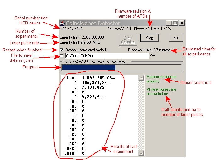
This simple application will run a set number of experiments before stopping and showing the results. The user sets the number of experiments (laser pulses) to run and its approximate rate. If the run is to be restarted then "Repeat" is checked. If the results are to be recorded in a file then the "File" box is checked. Hit "Start". A progress bar will show estimated time remaining. After the run does end, the results are shown. If the laser counted down to zero (the run was not manually stopped) then a notice will say that the "experiment finished properly". If the sum of all counters adds up to the requested number of experiments (laser pulses), then a notice will say that "all laser pulses are accounted for".
The results are shown in the binary weighted order of the APDs, i.e. Counters 0 to 15 for four APDs, or 0 to 63 for six APDs, plus the final laser count.
The file data is in CAVE format exactly as it appears in the GUI except without the commas in the numbers. Enter the file base name, each file is named with the run number as a suffix plus ".cave". In the example shown, the first file will be CoinDet1.csv, the second CoinDet2.csv and so on. Note that any existing files will be overwritten. To avoid overwriting previous data, append a series suffix to the file base name.
LED2 is turned on when the program starts. LED1 turns on when experiments are running.
Return to homepage
| Sorry, no more chance for asking direct questions, queries, broken links, problems, flak, slings, arrows, kudos, criticism, comments, brickbats, corrections or suggestions. |
|

|