

|
 Alan Stummer
Research Lab Technologist |
|

|
SPCM Coincidence |
")
|

|
Downloads
|
I am curious who uses what. Are these webpages a waste of time, or are they any help to others? Are the circuits, software and utilities appearing in other labs? Please send your comments or suggestions or what you have used (or not) or schematics of your version or pictures or anything! Email me, or be creative and send a postcard! I want to hear from the vacuum! |
Links
|
|
NOTICE: This webpage and associated files are provided for reference only. This is not a kit site! It is a collection of my work here at the University of Toronto in the Physics department. If you are considering using any schematics, designs, or anything else from here then be warned that you had better know something of what you are about to do. No design is guaranteed in any way, including workable schematic, board layout, HDL code, embedded software, user software, component selection, documentation, webpages, or anything. All that said, if it says here it works then for me it worked. To make the project work may have involved undocumented additions, changes, deletions, tweaks, tunings, alterations, modifications, adjustments, waving of a wand while wearing a pointy black hat, appeals to electron deities and just plain doing whatever it takes to make the project work. |
||

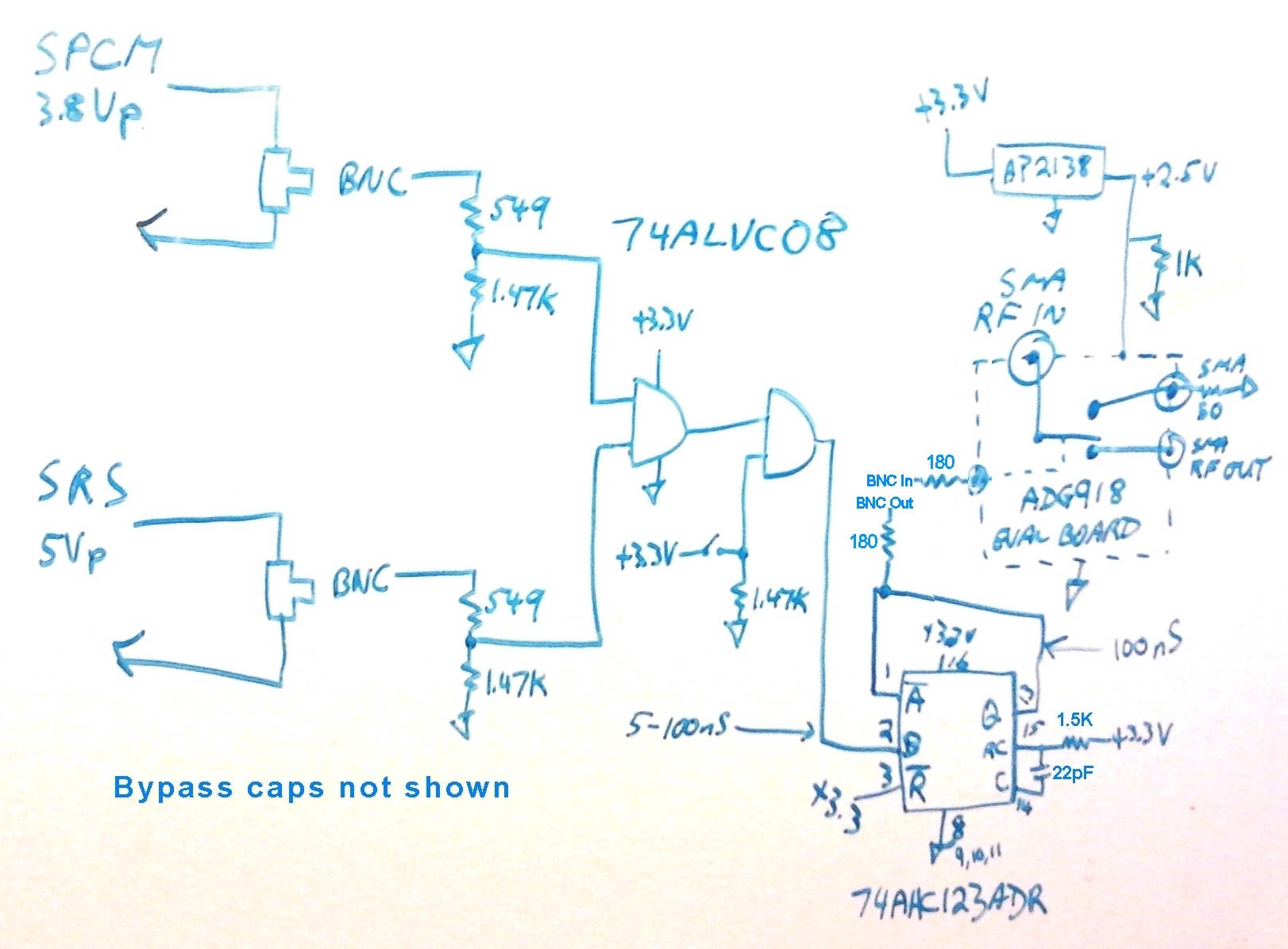
Started February 2014 for Amir in Aephraim's lab. A SPCM (Single Photon Counting Module) detects a photon which hopefully coincides with a pulse put out by the SRS timing generator. The SPCM output pulse is 20-100nS, module dependant. The SRS output is approximately 100nS. However, the SPCM is noisy and gives many false detections. This circuit logically ANDs the SPCM and SRS signals to identify valid photon detections. The AND output is used to interrupt an RF signal, purely as a way to detect the coincidence.
The hearts of the unit are a
SN74ALVC08Nquad 2-input AND running on +3.3V. Because both the SPCM and SRS have other duties and their
outputs are nominally 50 Ohm, a small part of the signal is tapped and attenuated to LVTTL levels to go into
the AND gate. The AND gate output is ANDed with a switch for enabling then sent to a 74AHC123 100nS one-shot
to ensure consistent pulse widths. The output from the ons-shot goes to a BNC to be put through an external digital
delay line. The delay line output goes back into the unit where it disables an RF switch, an ADG918 eval board
running on +2.5V. Finally, that RF switch passes through an externally sourced -10dBm 100MHz signal and back
out to a spectrum/IQ analyzer.
Return to homepage
| Sorry, no more chance for asking direct questions, queries, broken links, problems, flak, slings, arrows, kudos, criticism, comments, brickbats, corrections or suggestions. |
|

|