
| IN THIS ISSUE |
| FEATURES From the President Leading Edge Campus News Gifts Alumni News Letters Calendar Looking Back |
| OTHER ISSUES |
| HOW TO KEEP IN TOUCH |
| CONTACT US |
| SEND A LETTER TO THE EDITOR |
| ADVERTISING RATES |
| ADDRESS UPDATE |
| ALUMNI & FRIENDS |
| NEWS AND EVENTS |
| U of T HOMEPAGE |
Light heavyweights
A team of U of T scientists has won an international fight to control light and make it dance like electrons. A new era in telecommunications and computing is about to enter the ring
BY MICHAEL SMITH
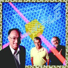 Sajeev John, left, Henry van Driel and Geoffrey Ozin: making light do anything electricity can – and then some Photography and Photo Imaging: Jim Panou |
It's only a speck of silicon, glinting with green-gold iridescence and smaller than a fingernail paring. Yet this tiny speck – so small it could be blown away by a sneeze – may hold the future of telecommunications, computing and perhaps even industries no one has yet imagined. It represents, in the purest sense of the word, a breakthrough. And it's both a technological beginning and the end of a remarkable scientific story – a tale that combines luck, brains, teamwork, experimental wizardry and deep theoretical insight all rolled up in one package.
The story could begin in 1987, when Sajeev John, a physicist who grew up in London, Ont., wrote a seminal paper in theoretical physics while an assistant professor at Princeton University. His topic? How to make materials that would cage light. Such materials would enclose photons, the particles of light, rather than electrons, and could be used to create circuits and switches that would use light, rather than electricity.
Or, if you take a long view, the story could begin in 1948 when William Shockley, Walter Brattain and John Bardeen created the first transistor. They later shared a Nobel Prize for their work, which led inexorably, as we all now know, to today's silicon-based society.
But for our purposes, let's take a closer starting point: The St. George campus of the University of Toronto, late in 1998. John, now in the physics department, is a guru of the new science of photonics. His theoretical insight is central to a worldwide drive to make light jump through the same hoops as electrons do – to make optical microchips, for instance, instead of electronic ones. And central to that endeavour are "photonic bandgap" materials that can cage light with a specific wavelength of 1.5 micrometres (the wavelength used in fibre-optic cables).
Electrons want to stay in wires, but light just wants to be free. Sure, with some engineering, you can confine light to a fibre-optic cable, but even then, a slight kink in the cable and the photons escape. Making light work, as we routinely make electrons work, requires a material that won't let photons escape.
The bad news was: no one had such a material. The good news was: John knew how to make it. All he needed were a top-notch materials chemist, an experimental physicist who understood photonics, and a source of exquisitely engineered artificial opal to serve as a template. As it turned out, all three came together dramatically over a period of a few months.
John's theory called for a lattice of air bubbles of a certain size, surrounded by silicon and joined by little silicon tunnels. Such a lattice of air bubbles, he theorized, would be completely opaque to light at 1.5 micrometres. Carefully engineered defects in the material could then create tracks along which photons would have to travel – wires for light. The problem was how to make such a lattice.
Here again, John's theory provided a blueprint. To make the lattice, you need to start with a template – a kind of negative image of the final structure. In technical terms, what was needed was an almost perfect array of tiny glass balls, arranged in what mathematicians call a face-centred cubic lattice. And that, chemist Geoff Ozin thought, was going to be tough.
Ozin has spent his professional life making new materials. Seated in his spic and span office in the chemistry building, under a black and white poster of John Cleese doing a Silly Walk, Ozin says: "That's what people like me do – we make stuff." Designing new materials is literally a family matter for Ozin; his father was a bespoke tailor near London's Savile Row and his sister worked for some of the top fashion designers in London. "It's in my genes," he says. "The esthetic that drives me to do what I do is clearly design."
But in late 1998 when John first approached him to work on a photonic bandgap material, Ozin was reluctant. He had been working – as many chemists do – on a scale of about 10-billionths of a metre, the so-called molecular scale. "What Sajeev was basically asking me to do was to jump from 10 nanometres to 1,000 – and he wanted it done in hurry," Ozin says. There was no doubt in Ozin's mind he could increase the scale 100 times; he had been finding ways to do chemistry on a larger scale for years. But the question was time. He figured it would take at least six months to learn how to make the opal templates, before he could even start figuring out how to make the silicon lattice. So he said no.
Half a block south, in his 10th-floor physics building office, John greets me from behind a desk crenellated with stacks of paper. He takes a nearby chair – a good thing since he'd be hidden from view if he sat at his desk – and immediately slides down onto his tailbone, legs outstretched and crossed at the ankles. It is about a month after he and his colleagues have published their landmark paper, "Large-scale Synthesis of a Silicon Photonic Crystal with a Complete Three-Dimensional Bandgap near 1.5 Micrometres," in Nature. Hidden in that rather ungainly title is all the excitement in the world, although John tries to be measured: "It certainly has the potential to be technologically like a revolution, in which you have photons entering technology the way the electron has done," he says. "It makes us feel like we're back in the 1940s, when the electronic semiconductor was being developed."
But late in 1998, John was still trying to find someone to make his lattice of air bubbles. He was in contact with a group of researchers in Spain – Francisco Meseguer and Cefe Lopez, with students Hernan Miguez, Marta Ibisate and Alvaro Blanco – who were making exquisitely engineered artificial opals. On the microscopic scale, an opal is an ordered array of tiny balls of glass – just what John ordered for his template. John told the Spanish that Ozin felt it would take too long to make the template. No problem, the Spanish researchers replied – we'll make the template, you get Ozin to make the lattice.
The templates and the chemistry weren't the only obstacles; John also needed someone to show that the material – once made – did in fact have a bandgap. Luckily, that person, physics professor Henry van Driel, was on the next floor up and eager to get involved, because he had worked on photonics with John for years. He, too, started to work on overcoming Ozin's reluctance. Van Driel remembers meeting with Ozin and his graduate student Emmanuel Chomski; Ozin said the work would take two years, Chomski said it would take two weeks. This was May 1999, so "it clearly wasn't two years," van Driel chuckles, although it did take the summer and most of the fall.
With Ozin on the team, John says, "Suddenly I knew I had all the things would need to translate this into reality." For van Driel, a key element of this story is teamwork. Grad students Jessica Mondia and Stephen Leonard and post-doc Serguei Grabtchak in van Driel's lab worked with Chomski and Ozin to test and refine the materials, in consultation with John and student Ovidiu Toader. Unfortunately, van Driel himself was sometimes out of the loop, because he was on sabbatical in Amsterdam.
Leaning against a cabinet in his lab, hands shoved into his pockets, van Driel surveys his young crew with pardonable pride: "The feedback was simply intense," he says, "and they did great work." It was also a defining moment for the young researchers – to be involved with a major project, in a race with competing scientists in other labs. "This might be a once-in-a- lifetime experience," van Driel says. Leonard, though, has a more down-to-earth description: It was like baking a cake. "You need a recipe, excellent supplies, good cooks and people who know how it should taste," he says. John had the recipe, the Spanish researchers had the supplies, and Ozin and Chomski were the cooks. And, Leonard adds, "We knew how it should taste."
The interplay of scientific theory and practice is rarely direct. It's not uncommon for theory to languish for years before an experimentalist does anything with it, and it's equally possible for an experiment to be carried out without any theory to explain what happened. But this story is different – at least partly because three of the four needed elements were within half a block of each other on the U of T campus. It's also different, Ozin says, because John's theory was remarkably detailed. "He laid out the road map for everyone – you had only to read the road map and if you had the chemistry, you could go and do it," Ozin says.
Of course, it wasn't simple. First, you needed the template – a precisely organized array of tiny glass balls (which is all that an opal really is). The balls all had to be exactly the same size – 870 nanometres in diameter – and they had to be packed together like oranges in a box. Like oranges in a box, there would be empty spaces between the balls. Unlike oranges, however, the glass balls also had to overlap each other just slightly, to be "necked." Without the necking, the opal template would fall apart, but more importantly, the necking is a key element of the final product: No necking, no bandgap. It was a tough recipe, but the Spanish group was able to do it.
The theory called for Ozin to deposit silicon throughout the opal, using a technique called chemical vapour deposition, coating each tiny ball layer by layer, so that precisely 86 per cent of the space between the balls was filled. Finally, using hydrogen fluoride, in what Ozin calls a "touchy" process, the chemists etched away the template, leaving a Swiss cheese of silicon.
Then van Driel's posse went to work. The idea of a bandgap is that the material will be opaque to certain wavelengths of light in all directions, unlike normal materials, which block some light in some wavelengths in some directions. But it's not enough to spray some silicon into some opal and say you've got a bandgap – you have to show it really won't let the light through in any direction. And that's what van Driel's team did: testing a sample, making suggestions to the chemists for refinements, testing again.
Finally, late in 1999, they had it – a material that could be made efficiently on a large scale, and that completely blocked l.5-micrometre light. The Canadian researchers had won an international race based on an unlikely combination of experimental and theoretical skills. Says van Driel: "Lots of people were trying to do this, but they were missing some part of the expertise."
It was a race run on a shoestring: John estimates they spent "several hundreds of thousands of dollars" on last year's experiments, compared with "several millions" that other groups were spending. And it was a race with a lot at stake: although John might modestly demur, the photonic bandgap material represents a scientific advance on the same scale as the semiconductor/transistor, which was worth a Nobel Prize in physics. But if the scientific story has ended in triumph, the technological story is just beginning. The advance could spawn a huge industrial complex. "We've won a race," says John. "But we've created a much bigger race."
Creating the photonic bandgap material was just the first step. Now comes the hard part: making it into devices, such as optical microchips, waveguides and microlasers. "There is," John says dryly, "a lot of engineering that lies ahead." But in theory, if you make the material, but introduce what Ozin calls "designer defects," you can make light do anything electricity can do and then some.
For now, all three researchers say, the key issue is to begin developing the optical technology made possible by the photonic bandgap material. Some of those technologies may include microlasers, microcircuits of light and all-optical switches, Ozin says. That green-gold speck of silicon could be the basis for a trillion-dollar industry. No longer reluctant, Ozin sees a whole world of new materials to be made, a whole new universe of possibilities both in photonics and elsewhere. "I'm reborn," he says. "Now I know what I want to do."
Whether the industry will be Canadian will depend on government and industry. Right now, John worries, other countries could be starting to capitalize on the U of T work and could leave Canada in the dust. Consider the transistor: It was invented in the United States, but the first to make money with it were the Japanese. Time will tell if the same thing happens to the photonic bandgap material – and time is short.
Michael Smith is a Toronto science writer.
| BACK TO TOP |
| | |
 | University of Toronto Magazine J. Robert S. Prichard Alumni House 21 King's College Circle, Toronto, ON Canada M5S 3J3 Tel: (416) 946-7575 Fax: (416) 978-5102 Web: www.magazine.utoronto.ca E-mail: uoft.magazine@utoronto.ca |