
"PhotoFinish" - Coincidence Timer
|
|
|
Downloads
|
I am curious who uses what. Are these webpages a waste of time, or are they any help to others? Are the circuits, software and utilities appearing in other labs? Please send your comments or suggestions or what you have used (or not) or schematics of your version or pictures or anything! Email me, or be creative and send a postcard! I want to hear from the vacuum! |
Links
|
Versions
|
|
NOTICE: This webpage and associated files is provided for reference only. This is not a kit site! It is a collection of my work here at the University of Toronto in the Physics department. If you are considering using any schematics, designs, or anything else from here then be warned that you had better know something of what you are about to do. No design is guaranteed in any way, including workable schematic, board layout, HDL code, embedded software, user software, component selection, documentation, webpages, or anything. All that said, if it says here it works then for me it worked. To make the project work may have involved undocumented additions, changes, deletions, tweaks, tunings, alterations, modifications, adjustments, waving of a wand while wearing a pointy black hat, appeals to electron deities and just plain doing whatever it takes to make the project work. |
|||
Many methods were investigated but the simplest was selected. The photons are each detected in APDs (Avalanche PhotoDiodes), call them PD1 and PD2. Upon arrival, PD1 is discriminated with a fast comparator, to define the timing demarcation on the relatively slow PD1 rising edge (~300pS). That comparator output goes into a simple 10nS RC integrator. A 100MSPS (100e6 samples per second) ADC (Analog to Digital Converter) reads the integrator voltage. By knowing the start and end RC values and the RC time constant (Tau), the time between the ADC sample and the actual PD1 event can be calculated. Early tests and backs of envelopes show that the start and end values are easy but that the RC time constant is the most critical.
Once the PD1 event has been detected, if the PD2 event occurs within about 1µS then it too is measured the same way. There will now be three pieces of information: the PD1 ADC value, the PD2 ADC value and the number of 10nS cycles between the two events - plus the ADCs' zero and asymptote values. This is enough to calculate the timing between the two events. If the PD2 event does not occur then no coincidence occurred, everything is reset and waits for the next event. This whole process is repeated with PD2 occurring first and waiting for PD1.
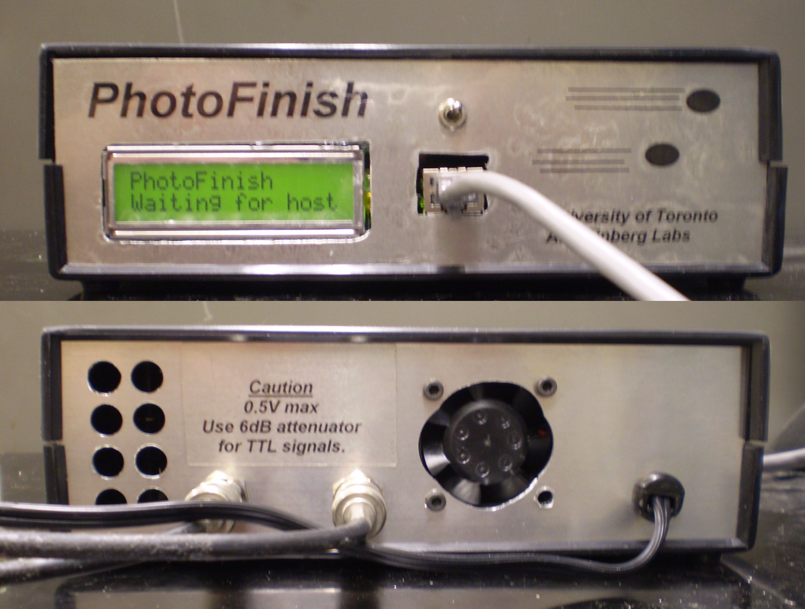
An Altera Cyclone II FPGA is used for the high speed real-time control of the ADCs, the timing measurement control and the interface to the microprocessor. FPGA firmware is written in Verilog with Altera's Quartus II. The microprocessor is a Rabbit Semiconductor RCM3200 module: complete with CPU, RAM, Flash, I/Os and TCP/IP. The Rabbit reads the ADC and timing information from the FPGA then transfers it to a PC or Mac for processing. The Rabbit software is written in C with Rabbit's Dynamic C. A test Gui, written in VB6, demonstrates the protocols and measures coincidences too.
The PCB is a standard 2-layer on 1.57mm (0.062") FR4 with 1oz. copper, using 0.18mm (0.007") trace and space. Vias - obviously no blind or buried vias - are finished to 0.43mm (0.017"), except power and plane connectors which are 0.63mm (0.025"). The top pour is the single ground. The bottom pour is also ground except for a +3.3V pour under the analog section and half of the FPGA. To minimize jitter and errors, the two input channels are layed out identically from the input to the analog side of the ADCs.
Please note that contrary to standard high speed and FPGA practice, a cheap 2-layer PCB is used: no buried supply and ground layers, no Rogers 4350 controlled dielectric, no solder mask, no silk screen. Regardless of what you have been taight, this works. Two boards arrived two days after the gerbers were sent out, for under (C)$200 including tax and shipping. The FPGA is in a QFP package so that it can be hand assembled: BGA packages cannot be hand assembled and may even have to be X-rayed if there are questions about the connections.
A single ground is used for both analog and digital. Except for the actual single-ended TTL inputs, all analog is differential so as to reduce common mode and grounding errors. Components are mostly top, although overflow bypass caps are on the bottom. The regulators are linear.
| Parameter | Conditions | Min. | Typ. | Max. |
|---|---|---|---|---|
| Input impedance | 50 Ohm | |||
| Input voltage | Positive voltages only | 0.0V | 0.4V | 1.0V |
| Input rise time | Jitter increases with rise time, prefer as fast as possible | 100pS | 500pS | |
| Time difference | B input relative to A input, limited by practical experimental range only | -1µS | +1µS | |
| Jitter | Emperical, data not used if either ADC < 650 or > 2350 (use about 90% of data) | ±50pS | ±65pS | |
| Capture rate | May be limited by user software and router/switch/hub | 0 | 37K/sec | |
| UDP/IP packet size | 100BaseT, coincidence report size in bytes | 9 | 954 | |
| Power consumption | +5V ±0.1V, includes display with backlighting but no fan | 1.07A | ||
| Ambient temperature | Untested outside of lab environment | 17° | 22° | 27° |
The last version of Altera's (Intel's?) Quartus IDE to support Cyclone II devices is 13.0sp1. Note that even 13.1 has dropped Cyclone II support. This link to Quartus II 13.0sp1 may or may not work, depending who owns Altera and phase of moon.
The last version of Digi's (Rabbit's?) Dynamic C IDE to support the RCM3200 module is 9.62. Good luck in finding it.
Since the PhotoFinish was made, Acam Messelectronic has come out with a family of ICs for time to digital measurement. If this project was to be spun then Acam's products would seriously be considered. Limitation of their parts are not yet known.
Xingxing's code rewrites were to increase the speed of coincidence detection. Much of the C was changed to assembler. If this project was to be spun then a faster processor would be considered. Candidates include Rabbit's RCM4xxx (double clock speed, minimal code rewiting) or a 16- or 32-bit processor from another vendor (more development time to develop infrastructure and code libraries, plus significant code rewrite).
| Sorry, no more chance for asking direct questions, queries, broken links, problems, flak, slings, arrows, kudos, criticism, comments, brickbats, corrections or suggestions. |
|

|

