 
|
 Alan Stummer Alan Stummer Research Lab Technologist |
|
|
Dual µWave EOM Driver |
||
 |
||

| Downloads |
I am curious who uses what. Are these webpages a waste of time, or are they any help to others? Are the circuits, software and utilities appearing in other labs? Please send your comments or suggestions or what you have used (or not) or schematics of your version or pictures or anything! Email me, or be creative and send a postcard! I want to hear from the vacuum! | Links |
NOTICE: This webpage and associated files is provided for reference only. This is not a kit site! It is a collection of my work here at the University of Toronto in the Physics department. If you are considering using any schematics, designs, or anything else from here then be warned that you had better know something of what you are about to do. No design is guaranteed in any way, including workable schematic, board layout, HDL code, embedded software, user software, component selection, documentation, webpages, or anything. All that said, if it says here it works then for me it worked. To make the project work may have involved undocumented additions, changes, deletions, tweaks, tunings, alterations, modifications, adjustments, waving of a wand while wearing a pointy black hat, appeals to electron deities and just plain doing whatever it takes to make the project work. |
||

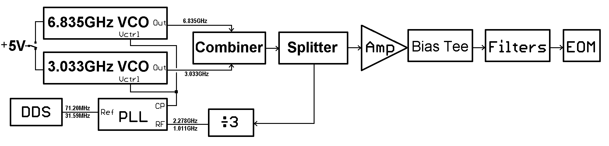
Started for Amir Feizpour in Aephraim's lab. Two commonly studied hyperfine transitions occur at 6.834682612GHz (Rb87) and 3.03257GHz (Rb85), give or take a few Hz. This project generates the drive signal for an EOM (ElectroOptical Modulator) to generate optical sidebands on a laser at either frequency. Each frequency has its own VCO (Voltage Controlled Oscillator) but share the other components.
Refer to the above block diagram. Only the 6.8GHz or 3.0GHz VCO is powered up at any one time. For the 6.8GHz path, a VCO, a Z-Comm CRO6835Z, generates the microwave RF at 6.835GHz. The RF is selected by a Minicircuits ZX10-2-722 2:1 splitter/combiner then split by another ZX10-2-722 2:1 splitter/combiner. One arm of that second splitter/combiner goes to the RF output amplifier. The other arm, used for frequency locking, is first dived by 3 by a Hittite HMC437MS8G to 2.278GHz then into the PLL. The PLL is an Analog Devices ADF4007 (eval board). It divides the 2.278GHz further by 64 to 35.60MHz. A DDS (Direct Digital Synthesis), such as the General Purpose DDS project, generates a reference frequency at about 71.20MHz for the PLL. The PLL first divides that by 2 to 35.60MHz then adjusts the VCO frequency to lock it to this reference. With the VCO locked, the 6.835GHz from the second combiner/splitter is amplified first by a Minicircuits TB-410-84+ (eval board for GVA-84+) then by a Hittite HCM870LC5 17.5dB 24dBm amplifier with a Minicircuit ZX85-12G bias-tee hanging off the output. Finally, the output may pass through bandpass and/or high or low pass filters before driving the EOM. Note that all of the components are on evaluation boards or connectorized modules so that this is a plug-and-play job for us with one 15V/1A wall wart and an assortment of POL LDO regulators.
The loop bandwidth is 8KHz with 50° phase margin. Although very low bandwidth, this centres the VCO's linewithout attempting to narrow it. It also allows enough bandwidth for sweeping. The loop bandwidth may be changed if it is too slow in future. The General Purpose DDS is used for the frequency reference.
For the 3GHz path, the 3GHz VCO (TBD) generates the microwave RF at 3.025GHz. After splitting and dividing by 3, it is at 1.01GHz before feeding back into the PLL. Otherwise, the 3GHz path is the same as the 6.8GHz path. Measured power output at 3.02GHz is adjustable between +15.1dBm (Vdd = +2.5V) and +21.3dBm (Vdd = +7.5V).
Return to homepage
| Please direct questions, queries, broken links, problems, flak, slings, arrows, kudos, criticism, comments, brickbats, corrections and suggestions to astummer_at_physics.utoronto.ca. |
|
 |