

|
 Alan Stummer
Research Lab Technologist |
|
|
Quad Analog Isolator 2 |

|
Downloads
|
I am curious who uses what. Are these webpages a waste of time, or are they any help to others? Are the circuits, software and utilities appearing in other labs? Please send your comments or suggestions or what you have used (or not) or schematics of your version or pictures or anything! Email me, or be creative and send a postcard! I want to hear from the vacuum! |
Links
|
|
NOTICE: This webpage and associated files are provided for reference only. This is not a kit site! It is a collection of my work here at the University of Toronto in the Physics department. If you are considering using any schematics, designs, or anything else from here then be warned that you had better know something of what you are about to do. No design is guaranteed in any way, including workable schematic, board layout, HDL code, embedded software, user software, component selection, documentation, webpages, or anything. All that said, if it says here it works then for me it worked. To make the project work may have involved undocumented additions, changes, deletions, tweaks, tunings, alterations, modifications, adjustments, waving of a wand while wearing a pointy black hat, appeals to electron deities and just plain doing whatever it takes to make the project work. |
||

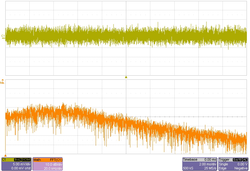
Started for Stefan Trotsky in Joseph's lab, Sept 2012. All four channels are identical. For each channel, the input voltage appears at the output, although the input and output are galvanically isolated. Each channel is also galvanically isolated from the other channels. The frequency response is DC to 40KHz (small signal).
There are eight CC1R5-1212DR-E DC-DC converters powered by a single wall wart power supply. The following applies to each channel seperately. There is one converter for the input stage and another for the output stage. Each converter is ±15V, 200mW load. The heart of each channel is a T.I. ISO124 analog isolator. The input voltage (relative to the input common), appears at the output (relative to the output common). Both the input and output sides are powered by separate ±15V. Because of the possibly large input-output offset, there is an offset adjustment. The output is buffered by a two pole low pass filter to reduce any residual switching noise from the isolation. A switch on the board can program channels 1-2 output for normal or inverted operation.
| Parameter | Value | Description and Conditions |
| Output impedance | 50 Ohms | |
| Output range | ±10V | No load |
| Output current | 4.5mA | Min, 8mA max |
| Frequency response - small signal | 41KHz | Up to 2Vp-p |
| Frequency response - large signal | 11KHz | Up to 10Vp-p, slew rate limited |
| Noise | 2mV | Even over spectrum |
Return to homepage
| Sorry, no more chance for asking direct questions, queries, broken links, problems, flak, slings, arrows, kudos, criticism, comments, brickbats, corrections or suggestions. |
|

|