 We have demonstrated the efficacy of thin-film photonic crystals for solar light trapping and electrical power generation.
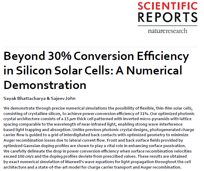
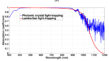
These photonic crystals consist of various (conical or inverted-pyramid) nano-pore arrays. These structures absorb more sunlight than a longstanding benchmark known as the Lambertian limit [Solar light trapping in slanted conical pore photonic crystals: beyond statistical ray trapping J. of Applied Physics 113, 154315 (2013)]. The novel underlying physics of these solar cell architectures comes from an effect known as Parallel-to-Interface Refraction and subsequent light-trapping in slow group velocity modes. Rather than making use of a photonic band gap, these solar cells rely on the ability of photonic crystals to greatly increase the electromagnetic density of states over selected frequency regimes.
We have demonstrated the efficacy of thin-film photonic crystals for solar light trapping and electrical power generation.
These photonic crystals consist of various (conical or inverted-pyramid) nano-pore arrays. These structures absorb more sunlight than a longstanding benchmark known as the Lambertian limit [Solar light trapping in slanted conical pore photonic crystals: beyond statistical ray trapping J. of Applied Physics 113, 154315 (2013)]. The novel underlying physics of these solar cell architectures comes from an effect known as Parallel-to-Interface Refraction and subsequent light-trapping in slow group velocity modes. Rather than making use of a photonic band gap, these solar cells rely on the ability of photonic crystals to greatly increase the electromagnetic density of states over selected frequency regimes.
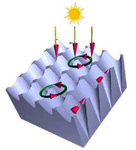
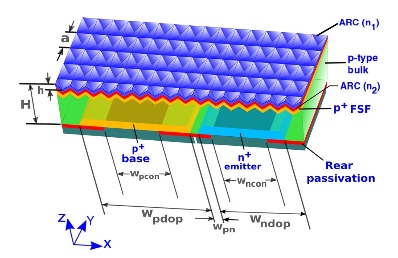
With only one micron (equivalent bulk thickness) of silicon it is possible to absorb nearly 85% of all available sunlight in the wavelength range of 300-1100 nm. This enables a one-micron thick silicon photonic crystal to achieve a power conversion efficiency of 17.5%, surpassing commercial silicon solar cells that use up to 300 microns of silicon. With 10-micron thickness of silicon it is possible to reach a photo-current density of 42.5 mA/cm2 (from sunlight in the 300-1100 nanometer wavelength range), not far from the 100% solar absorption limit of 43.5 mA/cm2. By including solar absorption over the full 300-1200 nm range and using an optimized doping profile that minimizes Auger and surface recombination, it possible to reach as high as 30% power conversion efficiency using a thin and flexible 10-micron-thick sheet of silicon. In a 15-micron-thick silicon solar cell with interdigitated back contacts, it is possible to achieve 31% power conversion efficiency, well above the world record of 26.7% and close to the Shockley-Queisser thermodynamic limit of 32.33%.
We have also shown near perfect solar absorption in ultra-thin-film Gallium Arsenide photonic crystals. With only 300 nm of GaAs, it is possible to absorb 99.5% of all available sunlight in the wavelength range of 300 nm- 860 nm. Using only 200 nm equivalent bulk thickness of GaAs, it is possible to realize a world record power conversion efficiency of 30% for a single-junction solar cell.
We are considering ways to improve the efficiency of Perovskite Solar Cells using light-trapping effects.