
Alan Stummer, Research Lab Technologist
n-Pulse Selector
|
|
|
|
| The PCB | A Pulse Transformer | Ringing in KD*P Pockels Cell |
|
NOTICE: This webpage and associated files is provided for reference only. This is not a kit site! It is a collection of my work here at the University of Toronto in the Physics department. If you are considering using any schematics, designs, or anything else from here then be warned that you had better know something of what you are about to do. No design is guaranteed in any way, including workable schematic, board layout, HDL code, embedded software, user software, component selection, documentation, webpages, or anything. All that said, if it says here it works then for me it worked. To make the project work may have involved undocumented additions, changes, deletions, tweaks, tunings, alterations, modifications, adjustments, waving of a wand while wearing a pointy black hat, appeals to electron deities and just plain doing whatever it takes to make the project work. |
||


- Previous attempts at this circuit used a planar triode based n-Pulse Selector.
- View list of all files
- Schematic and board in native Eagle format.
- Schematic in PDF format (might not be up to date).
Overview
Initially for Robin Marjoribank's lab, started Nov'05. In Dec'05, added the Piezo Driver project for Krister Shalm in Aephraim's lab. The same circuit and board is used in both projects, parts stuffed as required. The n-Pulse Selector variant is described below.
n-Pulse Selector
In a pulse train from a laser, a fixed number of pulses are to be selected, n number of pulses. This will trim off the weak pulses at the start and end of the train and leave a fixed number of clean pulses for the experiment. A pockels cell is used to switch the laser, either inside or outside of the oscillator or amplifier cavities. The switching has to be fast, under 5nS. To make it interesting, the pockels cell requires a change in differential voltage of 3-3.8KV to pass light. The proven methods are a planar triode, avalanche transistors and fast FETs, the latter two in banks to handle the voltage and power. This circuit is based on fast FETs.
Both sides of the pockels cell are biased to nominally 3.6KV through resistors of below 1M ohm. Differential voltage is zero and light is blocked. To each arm are stacks of FETs to ground. First the "on" stack is turned on and one arm of the pockels cell is near ground while the other remains above 3KV: differential voltage over 3KV and light passes. After the required delay, from 10nS to >1uS, the "off" stack is turned on and both arms of the pockels cell are near ground: differential voltage is zero and light is blocked again. After a few uS both stacks are turned off and the pockel cell returns to nominally 3.6KV. This return is slow due to RC delays caused by the parasitic capacitances.The FET chosen is Diodes Inc ZVN4424Z in the SOT89 (suffix "Z") package. Each stack has 16 rows of 2 FETs each. Each row is bypassed by a resistor to balance the quiescent voltage across the row. Adding more rows would speed up the switching due to lower voltage to drop across the Crss "Miller" capacitance, and adding more FETS in parallel would speed up switching due to higher current handling capacity of external parasitic capacitances. Both speedup fixes involve lots of FETs and 32 FETs per stack was decided on as a reasonable compromise.
So far this is fairly standard circuitry. The black magic comes in driving the FET gates. The gates are spaced 250V apart and need 10V drives. Any sort of divider stack would not only be tricky and messy but leave the FETs susceptible to the high dV/dt drain transients. Opto-couplers and off-the-shelf pulse transformers are slow as stink. Using coax as a pulse transformer can work, but not with 4KV isolation in a small size. Ferrites work well. A good article on the use of ferrites in broadband transformers is available from Fair-Rite. Tests with various sizes, styles and permeabilities showed that the Steward (now Laird) 28B0315-100 ferrite tubular bead will give a strong pulse to the gates with a fast rise time. The secondary is simply a 28AWG teflon wire going once through the [axial] core, connected between source and gate. Two rows share a ferrite, so the transformer has a dual secondary. The primaries are a 22AWG single teflon wire through the all of the cores, much like beading we did in kindergarden. An extra sleeve over the primary wire brings the isolation up to 4KV. The primary is connected to a 100V supply. The low side switches are four FETs in parallel. This driver stage is driven by a fast FET driver IC which translates the LVTTL control signal to a 11V swing. Working through the chain: the LVTTL trips the FET driver IC, which saturates the driver stage, 100V appears across the eight ferrite transformer primaries (12.5V per primary), 12.5V appears at each FET gate row and the stack saturates. Electrical tests show that the fall time is <<10nS.
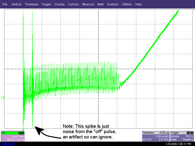
Although the ferrites make great pulse transformers, the pulse width is limited to about 100nS due to core saturation. However the pockels cell may have to be turned on for 1uS or more. When the "on" stack fires and after the ferrites saturate, the stack turns off. That side of the pockels cell starts it trip back to ~3.6KV following V PC = 3.6KV(1-e -t/RC), where RC = 50uS. To prevent this, the stack is fired for 30nS every 160nS, enough time for the ferrite to recover between the "keep-alive"pulses. This sustains the pockels cell differential voltage, as shown in electrical tests (done at reduced voltage so a normal 'scope probe can be used).
All timing and control is handled by the FPGA (see below). Asynchronous (AKA combinational) logic is used to for the leading edges to reduce synchronous timing lags. Delays from trigger input to the stacks are relatively long (~5-10nS) but stable with low jitter or drift. Both the 100V driver supply and the <4KV HV supply are controlled by DACs, as is the threshold for the trigger (photodiode) input. DAC control is described below.
At the core of the board is an Altera Cyclone EP1C3T100C6 FPGA. The same Verilog source code is used for both the n-Pulse Selector and Piezo Driver variants, although the latter ignores all of the HV stack triggering section of the former. A USB interface connects the board to the outside world. Dirvers are available for windows Visual Basic, C, and Labview. The USB sends a 16-bit control word to the board, the structure is 12 data bits, 3 command bits and one load bit. The sequence is to present the data and command with the load bit low, then toggle the load bit high then low. The command is executed on the rising edge of the load bit. There are no minimum or maximum timing requirements. For details of the commands, refer to the documentation at the start of the USB_Interface.v Verilog file.
Return to homepage
| Sorry, no more chance for asking direct questions, queries, broken links, problems, flak, slings, arrows, kudos, criticism, comments, brickbats, corrections or suggestions. |
|

|