-

- exfoliation_poster
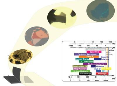
Recently mechanical exfoliation has received a great deal attention (2010 Physics Nobel) for producing single carbon sheets of graphene. However this method is incredibly flexible and has opened a new route to producing materials on the nanoscale. Materials with Nanometer thickness are an appealing platform for devices as well as exploring the roles of dimensionality, disorder, and free carrier density in complex materials. To this end we have produced exfoliated crystals of high temperature superconductors and topological insulators on a variety of substrates. I will discuss unique advantages of this technique as well as some of the challenges it posses. Interestingly we have observed subtle differences in the Raman spectra between the exfoliated and bulk crystals enabling noninvasive determination of thickness (Bi2Se3) and Doping level (Bi-2212).

